to the configuration shown on the schematic to prevent low-frequency audio detection by the AVC rectifier, therefore an audio output, when the AF GAIN control is set at minimum. If repairing the circuit shown below, recommend that same configuration be maintained.
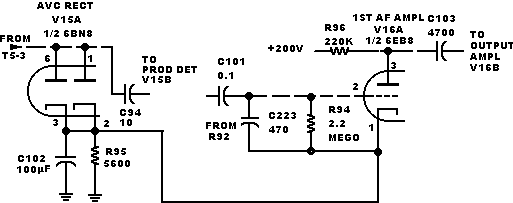
Changes made to the circult above to produce the circuit shown on the schematic are as follows: R210, 620 kW, added; C275, 0.01 µF, added; and cathode of V16A disconnected from cathode V15A and grounded. Reference part B of service bulletin no 8.
R213, 2.2 megohms; CR11, lN458; and C276, 0.05 µF, added. These changes reduce effects of strong adjacent channel SSB signals. If these components are not in the unit, they do not have to be added. Reference part C of service bulletin no 8.
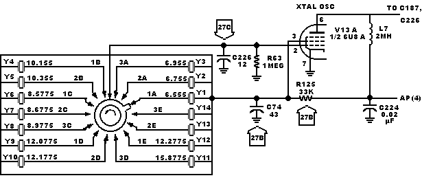
Y13, Y14, and Y18 thru Y31 are not furnished. These crystals are to be selected by the user.
Schematic diagram shows the KWM-2A crystal oscillator configuration. The crystal oscillator for the KWM-2 Is shown below.S14, S15, and Y18 thru Y31 are used only In the KWM-2A.
KWM-2 and KWM-2,A Transceivers. Schematic Diagram
figure 7-l (Sheet A)