-
Tune to 14.150 MHz, and set MIC GAIN As in step e.
Adjust C152 as in step f.
Tune 7.150 MHz, and set MIC GAIN as in step e.
Adjust C153 as in step f.
Tune to 3.700 MHz, and set MIC GAIN as in step e.
Adjust C154 as in step f.
Set OFF-ON-NB-CAL, switch to OFF
4.6.16 Receiving 455-KHz IF Alignment
Remove vfo tube V301 from socket, and set OFF-ON-NB-CAL switch to ON.
Set EMISSION switch to USB.
Connect signal generator to pin 8 of V17B, and set to 455 kHz. Increase signal generator output until S-meter shows slight indication (S3). Rock the signal generator frequency to center the signal at the approximate center of the filter passband.
Note If a vtvm is availahle, it may be connected to AVC bus and used as alignment peak indicator.
Adjust the slugs of L9 and T5 for peak indication on the S-meter. Reduce signal generator output as necessary to keep S meter indication low. Repeak L9 and T5 as in any standard alignment procedure.
replace vfo tube.
4.6.17 Receiver RF Gain and S-Meter Zero Adjustment
Set receiver to 14 MHz, and peak EXCITER TUNING control for maximum output. Set RF.
GAIN control (front panel) maximum clockwise position. Tune calibrated signal generator to same freque:n as receiver.Short RCVR ANT. jack J2 to ground: adjust S METER ZERO potentiometer Rl21 . S-meter so reads zero.
Remove short from J2. Using a 50 ohm ca1ibrated signal generator, apply 25 µV to the circuit shown in figure 41-3. Adjust RCVR GAIN ADJUST R132 until S-meter just moves off zero (1/2 S-unit or less).
Repeat step b.
This completes the laboratory alignment) the KWM-2/2A. Replace it in its cabinet.
4.7.1 Capacitor C10
Connect equipment as required to perform carrier balance (null) adjustment, paragraph 4.5.5.
Perform carrier balance adjustment.
Note In some units C10 may have to be added in parallel with C9 to produce the desired results.
If carrier balance adjustment does not produce an rf output of less than 0.2 Vrms select and replace C10 with a Value capcitor that provides less than 0.2 Vrms output.
Repeat carrier balance adjustment, pargraph 4 6.6.
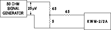
Receiver Gain Adjusment Setup
Figur 4-3